
Computer hardware explained: CPU (I)
The phones and computers we use every day all depend on a heart—the CPU. How can this tiny electronic component understand instructions, perform calculations, and even run complex games? Let’s take a look at the magic behind the CPU.
Author: emmm
Reviewed by: silverxz
In the introductory installment, we discussed how, whenever you double-click to open a program, calculate the sum of a set of numbers in a spreadsheet, or type a line in a document, the CPU is working behind the scenes, following the steps supplied by the software and executing instructions one after another.
But if you zoom in on the inside of a CPU, all you see are densely packed transistors and interconnections. It is hard to tell at a glance which parts perform calculations and which store data.
This naturally makes you wonder: how does a collection of metal and silicon with electricity flowing through it learn to “calculate” and “make decisions,” and then run a program step by step? To unravel the mystery, we first need to look at what lies at the very bottom of a chip.
I. Circuits that can do arithmetic
We normally do arithmetic in decimal, but in the world of circuits, reliably distinguishing between ten different voltages is not easy—even a little interference could make a “5” look like a “6.” An easier approach to implement is to distinguish between just two states: a higher range of voltages represents 1, called a high logic level, while a lower range represents 0, called a low logic level. A low logic level does not mean the power is off.
This is also an important reason why binary is widely used in computers. The smallest unit of information, which can take only the value “0” or “1,” is called a bit. Combine many bits, and the more bits there are, the larger the range of values they can represent. With an agreed encoding, they can also represent text and even program instructions.
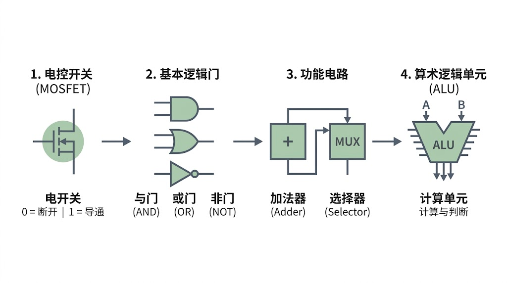
Once we have a way to represent numbers, how do circuits process these zeros and ones? The answer lies in a tiny component called a MOSFET (metal-oxide-semiconductor field-effect transistor).
We do not need to delve into its complicated semiconductor physics; we only need to think of it as a switch controlled by voltage. Take one common type of transistor as an example: with the appropriate connections, a sufficiently high voltage at the control terminal turns the switch on, while a sufficiently low voltage turns it off. Real chips use two types of transistors with complementary control characteristics together to reduce static power consumption. This is the basis of CMOS technology. Real circuits still have leakage, however, and switching also consumes energy.
A single switch can only determine whether current flows, but cleverly connecting several switches in series or in parallel lets us build basic logic gates that follow rules of logic:
NOT gate: an input of 1 produces an output of 0, and an input of 0 produces an output of 1. Its job is to output the opposite value.
AND gate: the output is 1 only when both inputs are 1. Think of it as “allow passage only when both conditions are met.”
OR gate: the output is 1 whenever at least one input is 1. Think of it as “allow passage when either condition is met.”
The rules of binary addition are simple: , , and (the subscript 2 indicates binary). When two ones are added, the current digit becomes 0, and a 1 is carried to the position on its left. First, consider adding two one-bit numbers, without a carry coming in from a lower position. We can split this into two tasks:
What happens to the carry?
Clearly, a carry is produced only when both numbers are 1—exactly what an AND gate already does.
What stays in the current digit?
The result is 1 when the two numbers differ and 0 when they are the same. In other words, “at least one must be 1, but they cannot both be 1.” Combine the AND, OR, and NOT gates we just discussed like building blocks, and this logic is easy to construct.
Package together the gates that calculate the current digit and the carry, and you get the simplest one-bit addition circuit, also called a half adder. To add multi-bit numbers, each position must also account for the carry from the position below it. Connecting circuits that can handle this carry produces a multi-bit adder.
Sometimes a circuit also needs to select one of several inputs—for example, choosing between the result of an addition and the result of a logic operation according to which is needed this time. This calls for a selector (MUX, or multiplexer). You can picture it as a railway switch: a control signal determines the switch’s position, letting the selected input pass through.
Combining adders, selectors, and various logic-operation circuits can produce an important component inside the CPU responsible for arithmetic and logic operations—the arithmetic logic unit (ALU).
II. How the circuits work together
With an ALU, our circuits can already add numbers and compare values, but the ALU itself does not remember the result of the previous step for the program. Programs often need to save intermediate results and then use the same arithmetic circuitry to carry out the following steps.
So we still need to answer two questions: where are results stored, and when are they updated? In common synchronous circuits, this requires registers and a clock. Let us use a simplified model to see how they work together.
A register is a fast-reading, fast-writing “scratch pad” inside a CPU core, right next to its arithmetic circuitry. It uses a feedback circuit structure to retain the zeros and ones currently stored while power is supplied normally. Intermediate results calculated by the ALU can first be stored in registers and quickly read out when later steps need them.
At this point, you might ask: if registers are so fast, why not make more of them? The storage cells, read and write ports, and interconnections needed for high-speed access take up chip area and increase power consumption. As the number of registers grows, the circuits that select and transfer data become more complex and may slow down access. Their number therefore cannot increase without limit.
So when should a register hold on to the old data, and when should it accept new data?
This calls for a clock signal to establish the update times.
Like a metronome, the clock signal repeatedly produces electrical pulses alternating between high and low levels. Here, one “beat” means a complete clock cycle, such as the interval from one rising edge to the next. A rising edge is the instant the signal changes from low to high. In this simplified model, the input registers update their data at one rising edge, and the arithmetic circuitry then performs its calculation. At the next rising edge, the registers that need to receive the results sample and store the data, which has already stabilized. The clock determines when updates occur, while the control circuitry determines which data to read, which operation to perform, and where to write the result.
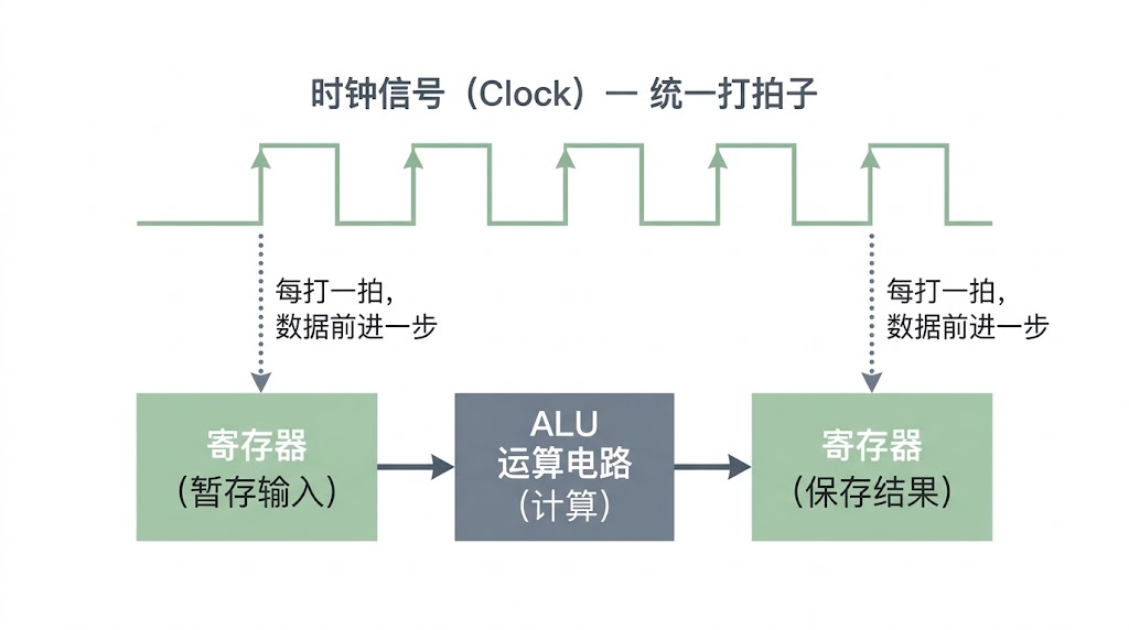
Note: The diagram illustrates how the clock, registers, and arithmetic circuitry work together. Taking two consecutive rising edges as an example, the first edge updates the input, the interval allows time for calculation, and the second edge saves the result.
When you shop for a computer or its components and see a specification such as 5 GHz, it refers to the clock frequency: when a CPU core runs at this frequency, it is equivalent to 5 billion beats per second. With other conditions, such as the average amount of work completed per cycle, held equal, a higher frequency generally means less time is needed to complete the same task. Performance also depends, however, on the average number of instructions completed per clock cycle, known as IPC (Instructions Per Cycle). We will discuss how frequency and IPC jointly affect performance in a later installment.
III. The complete journey of an instruction
Now the ALU that does the arithmetic, the registers that hold the working notes, and the clock that keeps time are all in place. We can finally return to the question left over from the introduction: how exactly does a CPU execute program instructions? Suppose you set up a simple rule in a spreadsheet: “Add the numbers in cells A1 and B1; if the total is greater than 100, carry out the step that highlights a warning in red.”
This rule ultimately requires many machine instructions to work together. To make the principle clear, we will focus on just a few actions—reading the numbers, adding them, making a comparison, and jumping conditionally—and explain them using a simplified CPU model. The program’s machine instructions are stored in memory. A special register inside the CPU called the program counter (PC) acts like a bamboo skewer pointing to a line in a recipe, helping the CPU keep track of where to fetch instructions next.
Suppose earlier data-loading operations have already read the values in A1 and B1 into registers. Next, let us follow the addition instruction through four basic stages. This is a process intended to make the idea easy to understand; it does not mean each stage always takes one cycle, or that all instructions follow exactly the same steps.
Fetch: using the address supplied by the program counter (PC), the CPU retrieves this addition instruction from memory. During sequential execution, the fetch position then advances to the next instruction.
Decode: the instruction just retrieved is encoded as a string of zeros and ones. As if consulting a dictionary, the instruction decoder recognizes it as an addition instruction and determines which registers to read the data from and which register to write the result to. The data participating in the operation are called operands.
Execute: following the decoding result, the control circuitry sends control signals that route the two operands from the registers to the ALU and tell the ALU to calculate their sum according to the rules of addition.
Writeback: the result travels along the writeback path and is stored in the specified destination register for subsequent instructions to use. If the program also needs to save the result to memory, an appropriate store operation performs that task.
After the addition is complete, later instructions still need to determine whether the sum is greater than 100. Based on the comparison result, the comparison and control circuitry decide whether to continue fetching instructions in their original order or update the PC to another address. If the condition is met, execution moves to the part of the program that highlights a warning in red. In this way, a program can choose different execution paths based on the results of its calculations.
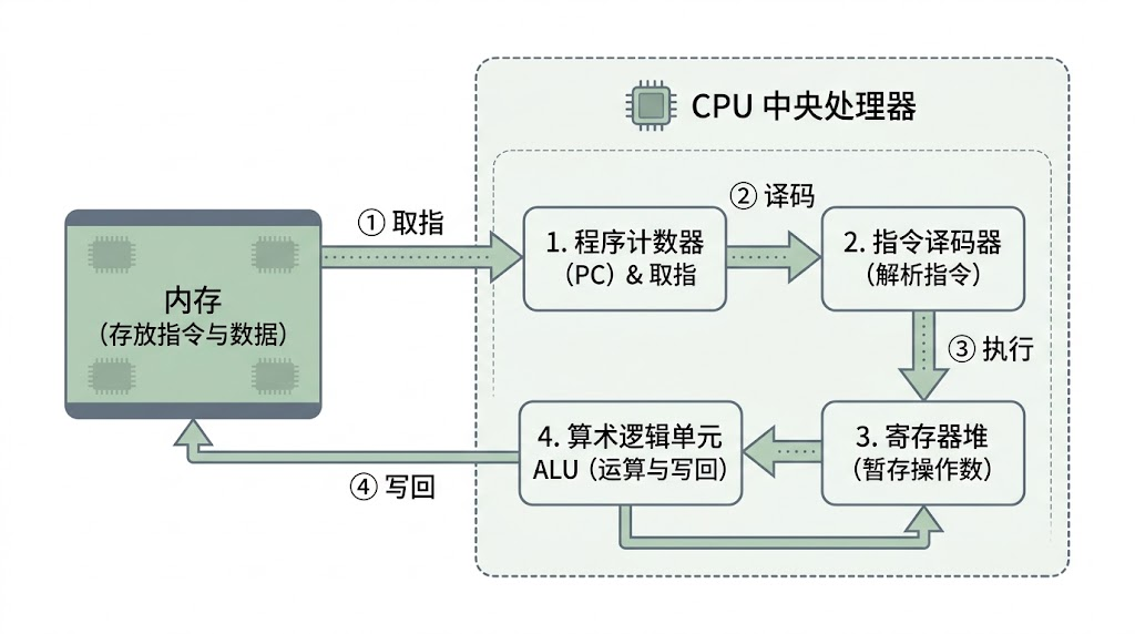
Note: The boxes in the diagram represent hardware components, while fetch, decode, execute, and writeback are stages in processing an instruction. The addition result in this example is written back to a register; writing to memory requires an appropriate store operation. A conditional jump changes the location of subsequent instruction fetching by updating the PC.
The CPU continually fetches instructions, interprets their meaning, and calls on the appropriate circuits to carry out operations. Executing large numbers of instructions in succession enables the various functions of software, games, and operating systems.
However, when we pull back from a single instruction, another problem appears:
We just saw that, when executing instructions, the CPU needs to obtain instructions and data. The problem is that the CPU’s internal clock ticks incredibly fast. From its perspective, data in a register is within arm’s reach, while a trip to memory is as slow as crossing half a city to collect goods from a warehouse. If all the required instructions and data have to be fetched from memory on demand, no matter how fast the CPU can calculate, it will still spend a considerable amount of time waiting.
How does the CPU solve this problem? What role does the cache play? Stay tuned for the next installment.
 爱发电(点击图片跳转)
Join the discussion
A question, a new idea, a different perspective.
Loading comments…